Biasing the (+) Op-Amp input with resistor to ground. Is its noise important?
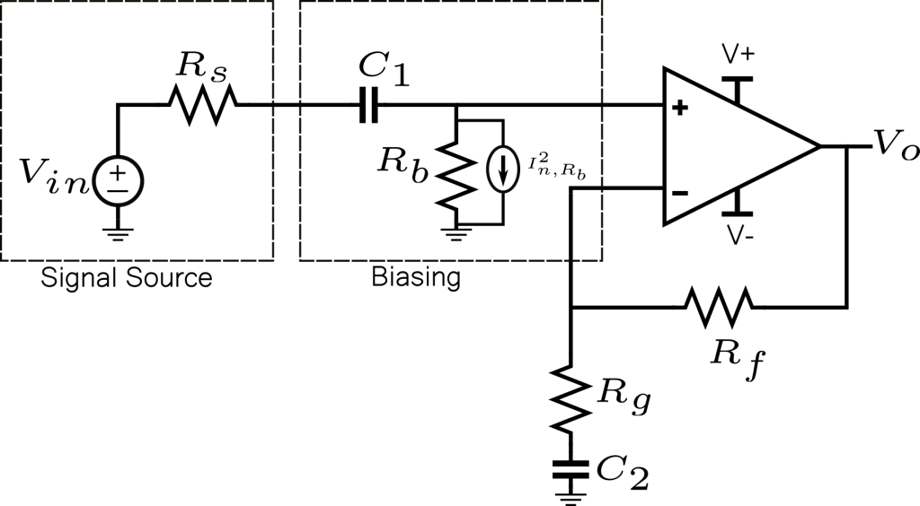
This article was inspired by two questions I read at electronics.stackexchange.com about the biasing the (+) input of an Op-Amp with a resistor to ground (\(R_b\) in the picture below).
One question asked about why it is needed and another one about the reason why its noise is negligible at high frequencies.
Even though the answers are given there, I thought these would be great examples to introduce a very simple circuit theorem that allows a simple computation of the input-referred noise of \(R_b\) (as seen in the picture above). This theorem can also be useful in other scenarios where you need to get some quick insight on input-referred noise contributions.
The theorem is a consequence of the KVL and KCL you’ve learnt in college. It allows to shift V- and I-sources around an schematic to help us simplify noise calculations. It was discovered by TH Blakesley back in 1894. Here is a link to the original article.
The I- and V-shift Theorem in Figures
The theorem can be easily explained with 2 pictures.
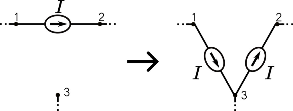

Explanation – Current Version
To explain the current version (I-shift from now on) of the theorem in figure one, we can write a the KCL for node 1 as follows (assuming currents flowing of the node as positive, and entering as negative):
\(0 = I + \cdots\)Similarly, for node 2:
\(0 = -I + \cdots\)You can see node 2 doesn’t know where the current is coming from, it simply knows that there is a current \(I\) entering the node. Likewise, node 2 doesn’t know where the current is going to, only that it is going out of it.
Therefore, we pick an arbitrary node 3 to redirect the current \(I\) flowing out of the node 1, and, at the same time, we send that same current \(I\) to node 2. We have to do this because node 3 didn’t have current \(I\) flowing in or out of it in first place. This akin to write add the following terms to the KCL expression in node 3:
\(0 = -I + I \cdots\)Explanation – Voltage Version
The voltage version (V-shift, from now on) simply reflects the fact that, if you write a KVL expression around a loop, a \(V\) exists in it, no matter where in the loop it is.
A more intuitive way to to understand this is to imagine placing a voltage meter at the right-end of each branch B, C and D in figure 2 (assume that \(V\) is grounded on its negative side). Obviously, we should measure a voltage \(V\) at any of those branches’ end. Therefore, we might as well assume that branch A is grounded and branches B,C and D have a voltage \(V\) each.
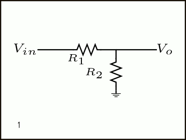
Resistive Voltage Divider – Input-Referred Noise
Any 1st year undergraduate student of electrical engineering knows how to calculate the transfer of a voltage divider. However, the noise is another story.

We want to calculate the input-referred noise density, i.e. the equivalent noise of the circuit at the \(V_{in}\) node. We know that the thermal noise power of each resistor is given by \(4kTR\), where k is the Boltzmann’s constant and T is temperature in Kelvin. Therefore, the total input-referred noise must include the total noise contribution of both resistors.
We can instantly recognize the noise power of R1 referred to the input is simply:
\(V_{n,R_1}^2=4kTR_1\)This is one term of the total noise contribution. However, obtaining the contribution of R2 is a bit more complicated.
Next, 2 ways to compute this noise will be shown; one that is more familiar using transfer functions, and another easier one using the current source shift theorem as presented above.
Calculating input-noise using transfer functions

The voltage noise of R2 must undergo 2 transfer functions before being referred to the input.
First, towards \(V_o\), the noise is transferred by \(\frac{R_1}{R_1+R_2}\) (that’s right, the resistive divider transfer seen from R2 as the input). Then, from \(V_o\) to \(V_{in}\), it is referred by the inverse of the original resistive divider transfer, i.e. \(\frac{R_1+R_2}{R_2}\).
Therefore, the input-referred noise contribution of R2 is:
\(V_{n,in,R_2}^2 = 4kTR_2\left(\frac{R_1}{R_1+R_2}\right)^2\left(\frac{R_1+R_2}{R_2}\right)^2 = \frac{4kT}{R_2}R_1^2\)From this expression, you might recognize that \(\frac{4kT}{R_2}\) is the equivalent current noise associated with R2. The method using the current noise of R2 instead of its voltage is shown in section below.
Calculating input- noise using the I-shift theorem

No better explanation than the GIF animation below to show the procedure of referring R2’s current noise back to the input as a voltage noise source.
As we learnt from the I-shift theorem in Figure 1, the current noise of R2 can be shifted and placed in parallel with R1, and another source must be added from \(V_{in}\) to ground (as shown in steps 3 and 4). This latter source can be discarded because it’s in parallel with the \(V_{in}\)voltage source. Therefore, in step 6, we are simply left with the voltage noise due to R2’s noise current times R1.
In short, we have arrived to the same expression above by doing a few manipulations in the schematic:
\(V_{n,in,R_2}^2 = \frac{4kT}{R_2}R_1^2\)Therefore, the total input-referred noise density of the resistive divider is:
\(V_{n,in,total}^2 = 4kTR_1 + \frac{4kT}{R_2}R_1^2\)Non-Inverting Op-Amp – Noise of Input Biasing
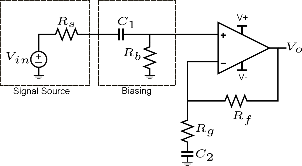
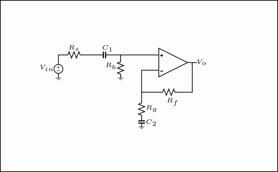
A typical non-inverting Op-Amp configuration is shown below.
\(R_s\) is the signal source impedance of the input voltage source, while \(C_1\) and \(R_b\) form a high-pass filter that isolates the amplifier from any DC coming from the source. \(C_2\) is added such that, at DC, it becomes an open and the amplifier becomes a unity-gain buffer. This is needed to avoid amplifying the voltage offset of the Op-Amp output by a \(1+\frac{R_f}{R_g}\) factor towards the output.
Why is \(R_b\) needed at all? This type of biasing is only needed if we are interested in amplifying non-DC components. Because of this, the only aim for \(R_b\) is:
To bias the (+) input of the Op-Amp at 0V.
There is also a good Analog Devices article that explains why the \(R_b\) resistor is needed, among other amplifier problems. However, they only give a vague statement about the noise \(R_b\) will contribute towards the input source.
Now, we are interested in the noise contribution of \(R_b\) referred to the input.
In the following subsection, the detailed (but easy) calculation of the \(R_b\)‘s input-referred noise in this configuration using the I-shift theorem.
\(R_b\) input-referred noise calculation
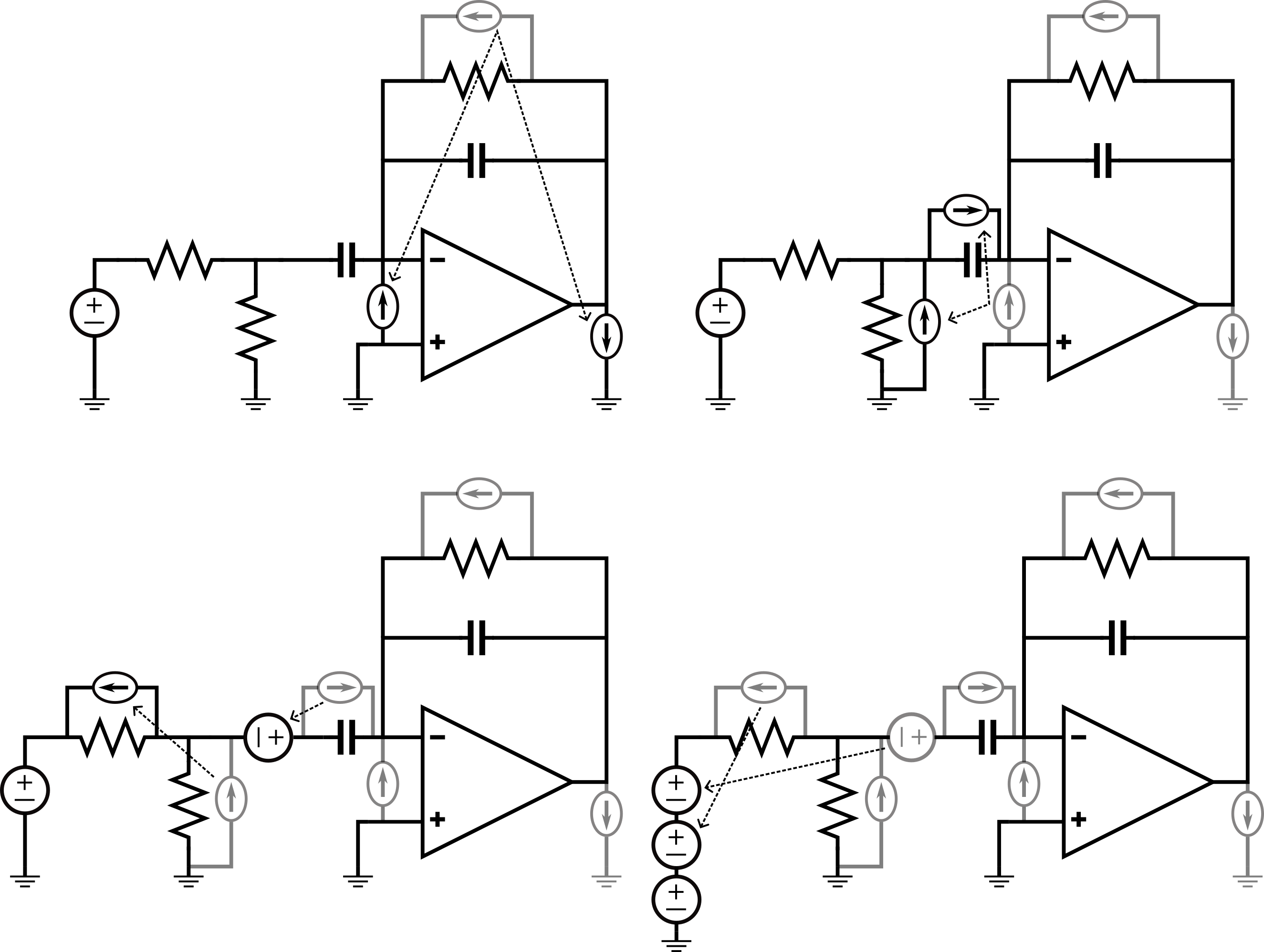
The current noise associated with \(R_b\) is given by \(I_{n,R_b}^2=\frac{4kT}{R_b}\) and can be modeled as a current source in parallel with the resistor itself, as shown in the figure below.
The current sources shifts and other steps are illustrated in the GIF animation below:
The 1-7 steps are described below:
- The \(I_{n,R_b}^2\) current noise source component associated with \(R_b\) is shown in parallel with it.
- The \(I_{n,R_b}^2\) now appears in parallel with \(C_1\)
- To comply with the theorem, we also need to draw \(I_{n,R_b}^2\) from \(C_1\)‘s left terminal to ground.
- The \(I_{n,R_b}^2\) component in parallel with \(C_1\) can be multiplied with each other to compute the equivalent voltage noise source \(I_{n,R_b}^2|Z_{C_1}| = \frac{4kT}{R_b}\left(\frac{1}{\omega^2 C_1^2}\right)\)
- The other \(I_{n,R_b}^2\) component drawn in step 3. can, again, be shifted to be in parallel with \(R_s\) and with another component from the left-terminal of \(R_s\) to ground.
- The \(I_{n,R_b}^2\) from the left-terminal of \(R_s\) can be eliminated simply because is in parallel with the ideal input voltage source. The component in parallel with \(R_s\) can be multiplied with the resistor to obtain an equivalent input voltage noise source of \(I_{n,R_b}R_s^2=\frac{4kT}{R_b}R_s^2\), just as we did in step 4. with the \(C_1\) capacitor.
- The \(I_{n,R_b}^2|Z_{C_1}|\) voltage noise source component calculated in step 4. can be simply shifted towards input since it is in series with \(R_s\), there is no transfer in between. Therefore, we finally have total noise contribution referred to the input due to \(R_b\), which is given by: \(\frac{4kT}{R_b}\left(\frac{1}{\omega^2 C_1^2}+R_s^2\right)\)
\(R_b\) input-referred noise calculation – Verification via Simulation
As a sanity check, I will use LTspice to verify the calculation performed in the previous section.
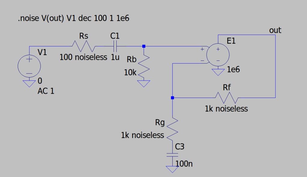
In order to isolate the noise contribution of \(R_b\), we use an ideal voltage-controlled voltage source with a gain of a million, while all the resistors (except \(R_b\)) are set to noiseless so that they don’t contribute to the input referred noise.
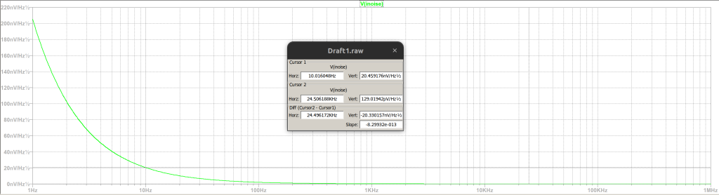
In Figure 10, we have have measured the noise at 2 frequencies, as shown in the table below:
| Frequency | Noise Measured |
| 10 Hz | 20.45 \(nV/\sqrt{Hz}\) |
| 24.5 kHz | 129.01 \(pV/\sqrt{Hz}\) |
As derived in the previous section, the input-referred noise voltage is given by:
\(V_{in,n,R_b}=\sqrt{\frac{4kT}{R_b}\left(\frac{1}{\omega^2 C_1^2}+R_s^2\right)}\)
| Frequency | Noise Measured | Noise Calculated |
| 10 Hz | 20.46 \(nV/\sqrt{Hz}\) | 20.48 \(nV/\sqrt{Hz}\) |
| 24.5 kHz | 129.01 \(pV/\sqrt{Hz}\) | 128.9 \(pV/\sqrt{Hz}\) |
The calculations match the simulations very well. The errors in the calculation are really small and are mostly due to rounding the frequency to the nearest decimal.
We can see that we need to make \(R_b\) as large as possible to reduce its input-referred noise contribution.
A question that might pop up is: But, if we make \(R_b\) larger, we are going to increase its voltage noise, how can we then understand, intuitively, that making it larger will reduce its noise contribution towards the input?
If we imagine that we had placed a noise voltage source in series with \(R_b\) to ground, we could notice that there is a voltage divider between \(R_b\) and \(R_s\) (assume \(C_1\) as a short for high frequencies). The transfer function is given by:
\(\frac{R_s}{R_s + R_b}\)Therefore, the smaller we make \(R_s\), or the large we make \(R_b\), the smaller this transfer from \(R_b\)‘s voltage noise source towards the input is. This also highlights the importance of knowing that the source impedance is small for our frequencies of interest for a low-noise design. Otherwise, we noise currents multiplied by the source impedance will be large.
Exercises
Capacitive Feedback Amplifier
Any operational amplifier with capacitive feedback needs their input and output nodes to be well-defined at DC. If the amplifier is standalone (i.e. doesn’t belong into the feedback path of another amplifier whose DC operating points are already well-defined), then, a resistor \(R_f\) in parallel with the feedback capacitor, as shown in the figure 11.
Derive the voltage input-referred noise expression due to \(R_f\), \(V_{n,R_f}^2\) . If we want to minimize \(V_{n,R_f}^2\), is it better to increase or decrease the value of \(R_f\)? The answer might surprise you!
Hints: Model the noise associated with \(R_f\) as a parallel current source and apply the current source shifting theorem. You can assume the \(V_{in}\) voltage source to be a short.

Have any comments/suggestions? Please them below!