In this article we will apply the voltage- and current-source shifting theorems explained in this other article.
We will work on several Op-Amp configurations to obtain its full input-referred noise expression. Each noise source in the op-amp configuration will be shifted to the input using the shifting theorems step-by-step.
- Non-Inverting Op-Amp Voltage Amplifier – Noise Analysis
- \(R_s\) – Source resistance.
- \(V_{n,R_L}\) – Voltage Noise of the Load
- \(V_{n,OA}\) – Input Voltage Noise of the Op-Amp.
- \(V_{n,R_g}\) – Voltage Noise associated with feedback resistor \(R_g\)
- \(V_{n,R_f}\) – Voltage Noise associated with feedback resistor \(R_f\)
- \(I_{n,OA}\) – Input Current Noise of the Op-Amp.
- Adding up all input-referred noise sources.
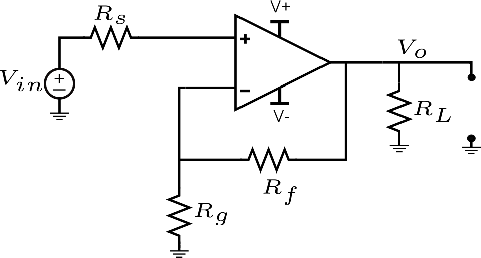
Non-Inverting Op-Amp Voltage Amplifier – Noise Analysis
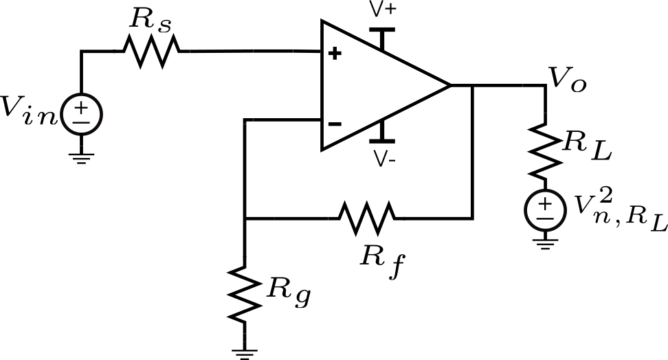
Figure shows a typical non-inverting op-amp voltage amplifier topology.
And in the following figure the same circuit topology is shown with the noise sources associated with each component.
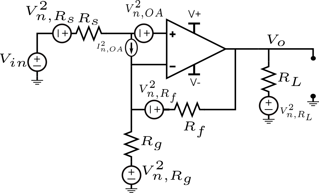
In each following subsection we will discuss how to refer each noise source to the input, such that we can compute the total input-referred noise of the circuit. An advantage of this approach, over, e.g. this article from TI is that you can obtain each noise source contribution’s directly at the input, without doing the cumbersome math of dividing every single term output noise term by the gain of the amplifier.
In the following analysis, we will assume the gain factor \(A=\frac{R_f}{R_g + R_f}\), the well-known gain of a non-inverting Op-Amp voltage amplifier.
\(R_s\) – Source resistance.
The source resistance has a noise power spectral density (PSD) associated with it given by \(V_{n,R_s}^2=4kTR_s\). Since it is located at the input, it is already input-referred. Easy.
\(V_{n,R_L}\) – Voltage Noise of the Load
Assuming we have a resistive load, it is bound to have a noise PSD given by \(V_{n,R_L}^2=4kTR_L\). TL;DR: it does not contribute noise when we assume an ideal Op-Amp.
An incorrect reasoning and conclusion might be that this noise source is simply referred back to the input by the voltage gain of the amplifier squared, i.e. \(\frac{V_{n,R_L}^2}{A^2}\), where \(A=\frac{R_g}{R_g+R_f}\).
This is incorrect because \(V_{n,R_L}^2\) undergoes one transformation before reaching the voltage output node \(V_{o}\). Namely, voltage division with respect to output impedance of the Op-Amp.
If we model, the output impedance of the amplifier as \(Z_o\) in series with its controlled source \(V_c\). If we use superposition, we can write the following expression for the output voltage node.
\(V_o=V_{n,R_L}\frac{Z_o}{Z_o+R_L} + V_c\frac{R_L}{Z_o+R_L}\)Since we have assumed that the Op-Amp to be ideal, then \(Z_o=0\). Thus, \(V_{n,R_L}\) contributes no noise to the output node of the amplifier; there is no need to refer it back to the input.
Nonetheless, other questions may arise, such as:
- We know \(Z_o\approx 0\) at DC in a real feedback amplifier, but this value increases as loop gain decreases at high-frequencies (for a shunt feedback configuration at the output, like the non-inverting voltage amplifier does), does that mean at high frequencies the load can contribute noise? The answer is yes, we could call it out-of-band noise.
To conclude, under the assumption of an ideal op-amp (infinite gain at all frequencies, thus 0 output impedance), the load resistance \(R_L\) contributes no noise to the input.
\(V_{n,OA}\) – Input Voltage Noise of the Op-Amp.
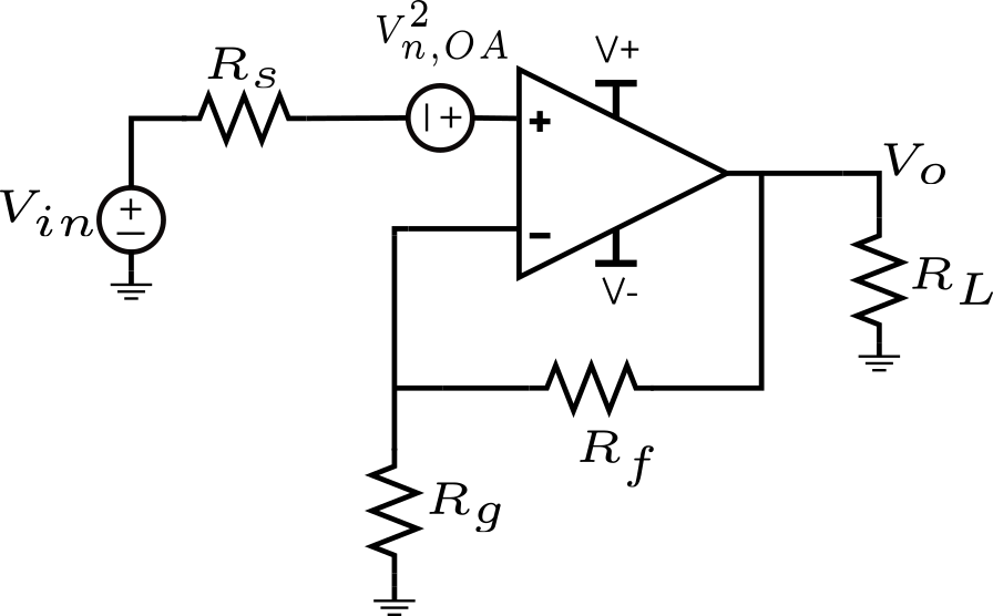
This noise source is directly in series with the input source (just like \(R_s\)); therefore, it is easy to see that it’s already input-referred. It simply adds to the noise the input source \(R_s\) produces.
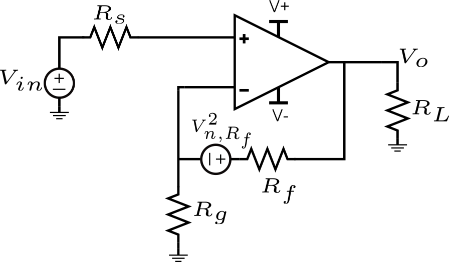
\(V_{n,R_g}\) – Voltage Noise associated with feedback resistor \(R_g\)
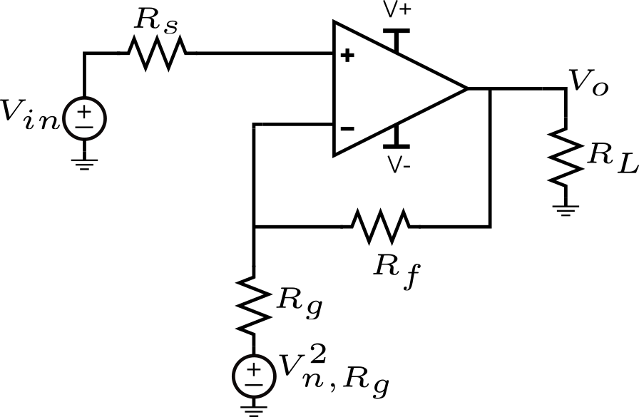
This noise source, as shown in figure 6 can be input-referred in many ways.
- Common way: recognize that \(V_{n,R_g}^2\) can be shifted to \(V_o\) via the transfer \(\left(-\frac{R_f}{R_g}\right)^2\) and then be referred back to the input via the non-inverting transfer \(\left(\frac{R_g}{R_f+R_g}\right)^2\). Multiplying every factor we obtain: \(V_{n,R_g}^2\left(-\frac{R_f}{R_g}\right)^2\left(\frac{R_g}{R_f+R_g}\right)^2\). Simplifying, we can arrive at \(V_{n,R_g}^2\left(\frac{R_f^2}{(R_f+R_g)^2}\right)=4kTR_g\left(\frac{R_f^2}{(R_f+R_g)^2}\right)\)
- An alternative way is shown in figure 7. Each of the 5 steps are explained as follows:
- Amplifier schematic with the \(V_{n,R_g}^2\) source modeled in series with \(R_g\)
- \(V_{n,R_g}^2\) is shifted over the ground node, appearing in 3 new places: in series with the input source \(V_{in}\) , the load \(R_L\) and the ground reference of the output node \(V_{o}\). Mind you, all of the 3 new resulting sources are fully correlated. We’ll come back to this later.
- The \(V_{n,R_g}^2\) in series with \(V_{in}\) is already input-referred. Nothing to do about it, just consider that it has a negative sign compared to the input source. The other source in series with \(R_L\) can be neglected in the same way \(V_{n,R_L}^2\) could be neglected. The last source appearing in the ground reference of the output node \(V_{o}\) can be shifted through the open to, finally, appear at \(V_{o}\).
- The \(V_{n,R_g}^2\) source appearing directly at \(V_{o}\) can be referred to the input by \(\frac{1}{A}\) to the input.
- Finally, we have the contributions of \(V_{n,R_g}^2\) in series at the input. As mentioned in point 3, their contributions are fully correlated; therefore, we add them as \(V_{n,R_g}^2(\frac{1}{A}-1)^2\) (taking care of the signs).
Simplifying the last expression obtained in point 5: \(V_{n,R_g}^2(\frac{1}{A}-1)^2\), we obtain:
\(V_{n,R_g}^2(\frac{1}{A}-1)^2=4kTR_g\left(\frac{R_g}{R_g+R_f}-1\right)^2=4kTR_g\left(\frac{R_f^2}{(R_g+R_f)^2}\right)\)Which is exactly the same as the common way of referring to the input, as it must be.
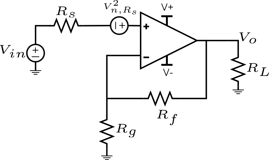
\(V_{n,R_f}\) – Voltage Noise associated with feedback resistor \(R_f\)
The \(V_{n,R_f}^2\) noise source is modeled in series with \(R_f\), as shown in figure 8.
A quick conclusion one might arise is that the \(V_{n,R_f}^2\) source might be shifted to the output, and thus can be easily referred to the input with \(\frac{1}{A}\). While this is correct, there is an extra voltage source we are forgetting.
According to the voltage shift theorem, when we shift a voltage source through a node, this voltage must appear in all other branches connecting to a node. This shifting process is shown in steps 1 and 2 in figure 9 below.
So what’s up with this extra \(V_{n,R_f}^2\) directly in series with the Op-Amp output? In step 3 shown above in figure 9, it says that we can simply neglect it. Why?
This is because, as the op-amp is ideal, the voltage gain of this Op-Amp is infinite. Therefore, any voltage source directly at the output of the Op-Amp must be referred to the input as 0 due to the infinite Op-Amp voltage gain.
Therefore, this noise source is referred to the input as \(\frac{V_{n,R_f}^2}{A^2}=4kTR_f\frac{R_g^2}{(R_f+R_g)^2}\)
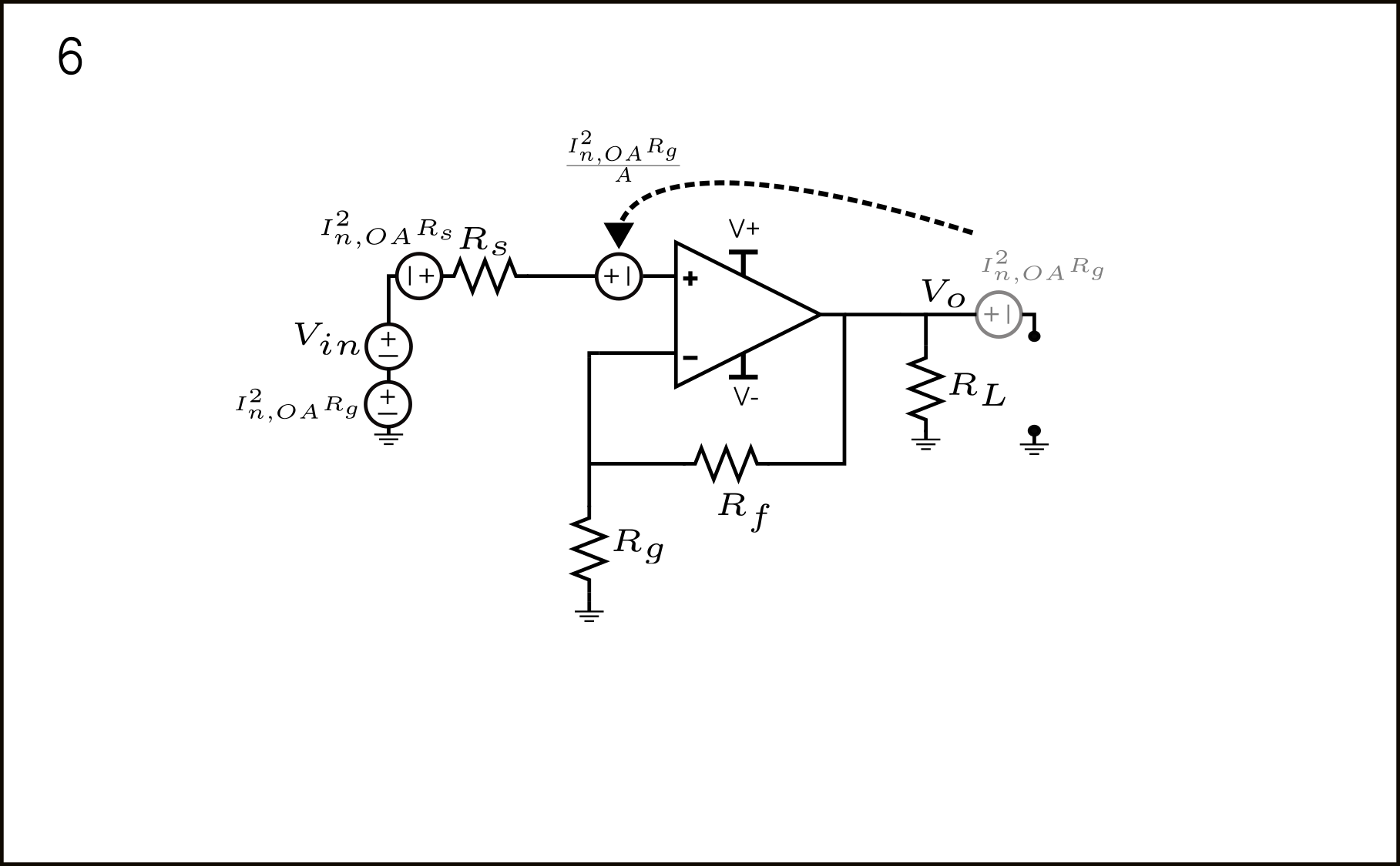
\(I_{n,OA}\) – Input Current Noise of the Op-Amp.
The input current noise of the Op-Amp can be modeled as shown in figure 10.
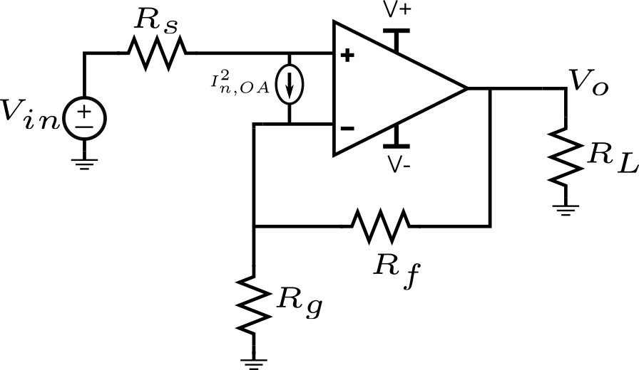
This is probably the hardest one to refer to the input, but via the current and voltage source shifting theorem, the procedure becomes more manageable. Each step is shown in figure 11.
- The Op-Amp shown with its equivalent input current noise.
- Using the current-source shifting theorem, we obtain new current sources from the (+) input of the Op-Amp to ground, and from ground to the top of resistor \(R_g\). Mind you, again, all these current sources are correlated. We’ll come back to this later.
- The source from the (+) input of the Op-Amp to ground can shifted, thus appearing across \(R_s\) and \(V_{in}\). The current source across \(V_{in}\) simply disappears, as only \(V_{in}\) can define a voltage between ground and tje (+) Op-Amp input, and can provide any current. On the other hand, the current across \(R_s\) simply produces a voltage \(I_{n,OA}^2R_s\). The current source across \(R_g\) simply produces \(I_{n,OA}^2R_g\) 1.
- Source \(I_{n,OA}^2R_g\) can be shifted through the ground node, thus appearing in 3 different places. The \(I_{n,OA}^2R_g\) in series with \(V_{in}\) is already input-referred. Nothing to do about it. The other source is in series with \(R_L\) The last source appears in the ground reference of the output node \(V_{o}.\).
- The source at the ground of node \(V_{o}.\) can be shifted through the open to, finally, appear at \(V_{o}\). The source in series with \(R_L\) can be neglected in the same way \(V_{n,R_L}^2\) could be neglected. The last source appears in the ground reference of the output node \(V_{o}\) can be shifted through the open to appear directly in series with the \(V_{o}.\) node.
- The \(I_{n,OA}^2R_g\) source appearing directly at \(V_{o}\) can be referred to the input by \(\frac{1}{A}\).
- Finally, adding up all the sources in a correlated manner, we have: \(I_{n,OA}^2\left(R_s + R_g – \frac{R_g}{A}\right)^2\).
Simplifying the expression obtained in step 7, we arrive at:
\(I_{n,OA}^2\left(R_s + R_g – \frac{R_g^2}{R_g+R_f}\right)^2=I_{n,OA}^2\left(R_s + \frac{R_gR_f}{R_g+R_f}\right)^2\)Adding up all input-referred noise sources.
To conclude we sum the contributions of all noise sources referred to the input:
\(V_{n,in}^2 = 4kTR_s + V_{n,OA}^2 + I_{n,OA}^2\left(R_s + \frac{R_gR_f}{R_g+R_f}\right)^2 + 4kTR_f\frac{R_g^2}{(R_f+R_g)^2} + 4kTR_g\left(\frac{R_f^2}{(R_g+R_f)^2}\right)\)Further simplifying, we arrive at the expression:
\(V_{n,in}^2 = 4kTR_s + V_{n,OA}^2 + I_{n,OA}^2\left(R_s + \frac{R_gR_f}{R_g+R_f}\right)^2 + 4kT\frac{R_fR_g}{R_f+R_g}\)Finally, some comments are in order:
- The input-referred noise depends on the source resistance. A high source resistance can lead to a high input-referred noise due to the Op-Amp’s intrinsic current noise.
- The noise contribution by the feedback network can be readily modeled by the parallel combination of the feedback network resistors, as \(4kT(R_g||R_f)\). Furthermore, the Op-Amp’s current noise is also reflected via the product of it and \(R_g||R_f\).
- It’s obvious that an smaller resistor will reduce noise, but it’ll do so at the expense of power consumption (in this case, more current will have to be consumed by the Op-Amp to drive the feedback network).
- For example: the power required by the Op-Amp to drive the feedback network (neglecting \(R_L\) and assuming infinite \(R_{in}\) of the Op-Amp) is given by \(P_{out}=\frac{I_{out}^2}{R_f+R_g}\). If we make a copy of this whole amplifier, and connect each copied to node to its original node, and assuming the Op-Amp current noise is negligible, the voltage noise contribution of the feedback network will be reduced by 3dB while the power consumption will be doubled (i.e. \(V_{n,\textrm{feedback network}}=\sqrt{4kT\frac{R_fR_g/4}{R_f/2+R_g/2}}=\sqrt{\frac{1}{2}}\sqrt{4kT\frac{R_fR_g}{R_f+R_g}}\) and \(\sqrt{\frac{1}{2}}=-3dB\)). This is a fundamental noise and power trade-off, for 2x the power, you get -3dB noise reduction.