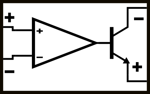
While the 3-terminal op-amp symbol is the most widely used active element used in textbooks to analyze circuits using feedback, it is limiting in the sense that no series feedback can be applied at the output. While most textbooks use a transistor (thus, already suggesting a particular implementation) to implement the 4th terminal, it is cleaner and useful to abstract away the whole amplifier before suggesting a particular implementation of it.
A universal active element that can accommodate series feedback at the output (as well as all the other types of feedback used around a 3-terminal op-amp symbol) is the nullor.
The nullor was first denominated as such by H. Carlin and D. Youla back in 1961 (See Reference section at the end of the article).
Definition of the Nullor
The nullor is a useful 4-terminal active element abstraction which is made of a nullator and a norator, which make the nullor suitable for circuit analysis. They can be thought of ideal circuit blocks that provide constraints to the nullor. They are not really abstracting a real circuit implementation individually. In addition, they only make sense when used as a pair. Theoretical circuits using an unequal number of nullators and norators are possible but not realizable.
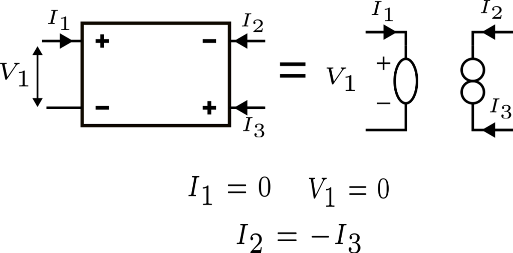
The equations in Figure 2 describe the nullor functionality. \(I_1=0\) and \(V_1=0\) might remind most readers of the op-amp golden rules, namely:
- No current flows into the input terminals of the op-amp
- Both input terminals are the same potential. Or, their difference equals 0 volts.
These constraints are set by the nullator element.
The third equation simply imposes that the \(I_3\) and \(I_4\) are the same (with the opposite sign), while the voltage across it is arbitrary. This is what we need the norator for. It should be noted that, while it looks like it complies with the function of a short circuit, it cannot be replaced by a short circuit. An example later will demonstrate this.
If we were draw the \(I_3\) backwards in Figure 2, one can intuitively understand that the current flowing through the top-right port must be equal to the current coming out of the bottom-right port.
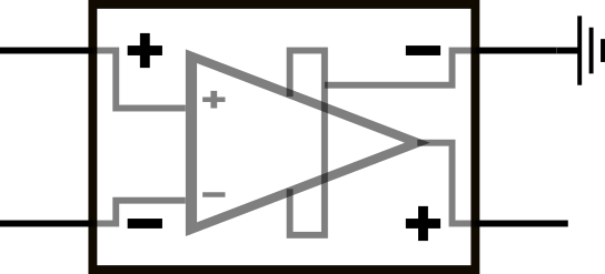
If we ground one of the terminals, it will have the exact functionality of a typical op-amp symbol:
Solving Circuits with the Nullor
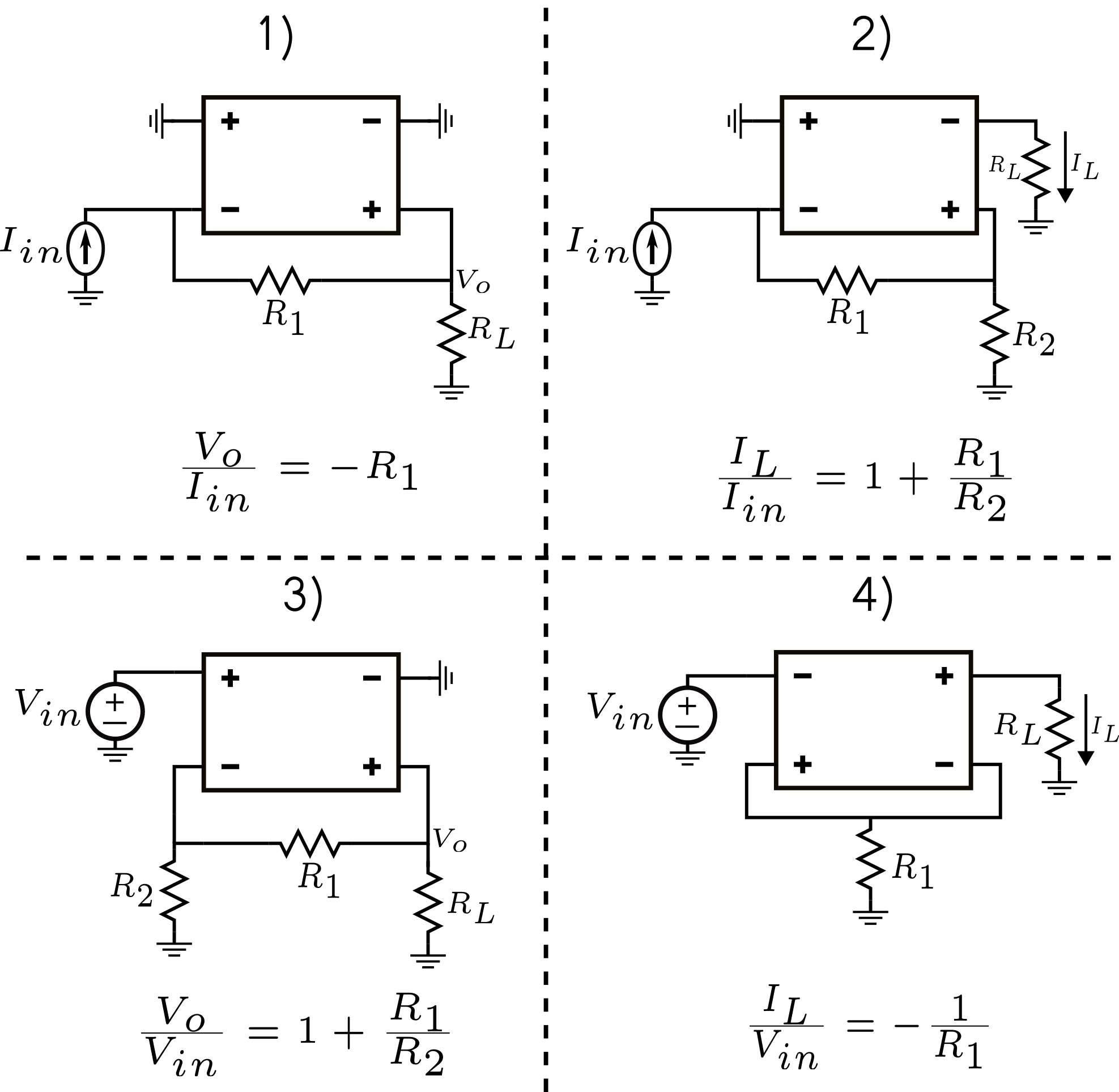
The nullor can be used in a variety of high-level circuit abstractions that can guide the amplifier’s implementation:
To keep this article short, only the current-to-current amplifier will be solved, as it is the most unusual circuit out of the 4 basic topologies. The circuit will be solved in 2 ways.
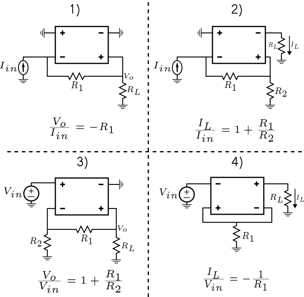
Solving Current-to-Current Amplifier – Method I
- Write 2 KCL expressions for node \(V_1\) and virtual ground (0V).
- \(\frac{V_1}{R_1}+\frac{V_1}{R_2}-I_L = 0\)
- \(I_{in} – \frac{V_1}{R_1} = 0\)
- Solve for \(V_1\) in (2) and obtain \(V_1=I_{in}R_f\).
- Replace \(V_1\) by the expression obtained in step 2 into equation (1) and solve for \(\frac{I_L}{I_{in}}\)
- Finally, derive:
- \(\frac{I_L}{I_{in}} = 1+\frac{R_2}{R_1}\)
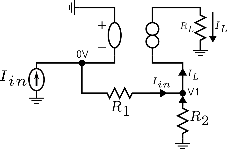
Isn’t the norator the same as a short?
It should be noted that, if, mistakenly, we assume the norator is a simple short, then, the first KCL expression:
\begin{align}
\frac{V_1}{R_1}+\frac{V_1}{R_2}-I_L = 0
\end{align}
would actually be:
\begin{align}
\frac{V_1}{R_1}+\frac{V_1}{R_2}+\frac{V_1}{R_L} = 0
\end{align}
We could say that \(V_1/R_L\) is \(I_L\). And we would get the same expression, but with the opposite sign. However, this brings the following issues:
- Despite having labeled \(V_1/R_L\) as \(I_L\), this does not change the fact that, now, \(I_L\) depends on the value of \(R_L\) itself since there is current division across 3 resistors: \(R_1,R_2\) and \(R_L\).
- \(V_1\) now depends on the \(R_L\)
A current amplifier must provide the current defined by its feedback network and not by its load. Clearly, modeling the nullor as such results into a defective feedback amplifier.
Solving Current-to-Current Amplifier – Method II
An easier way to solve this is to recognize that \(I_L\) is divided into \(I_{in}\) and the current through \(R_1\). Therefore, if we wanted to find the current flowing through \(I_{in}\), we can write:
\begin{align}
I_{in} = I_L\frac{R_2}{R_2+R_1}
\end{align}
From there, it’s trivial to solve for \(\frac{I_L}{I_{in}}\).
A More Complex Feedback Amplifier
From Figure 4, we can see that the V-to-I amplifier (topology 4) has a negative transfer. We will call it a transadmittance amplifier from now on.
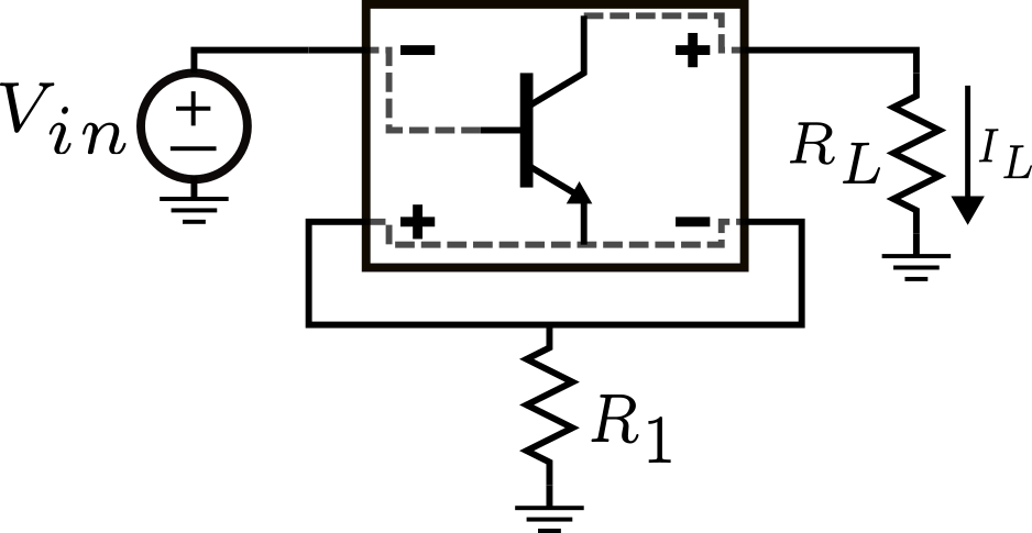
As an aside, one might be able to recognize that such a circuit can be implemented by the so-called common-emitter voltage amplifier.
The transfer is the same. The only thing to be added is that the current produced is now multiplied by the load (in this case, a predictable one chosen by us) to make a voltage.
However, What if we wanted to realize positive transadmittance transfer?
To achieve this, we can make use of the powerful nullor abstraction to come up with a non-inverting transadmittance concept.

The 1st step is to recognize that the direction of the \(I_L\) is positive. We need to implement something that takes a current in, and inverts it to a voltage of the same sign as the input voltage.
One way to do this is to use a transimpedance amplifier (I-to-V amplifier). If the current at the input of this transimpedance amplifier is “going out” (or has a negative sign), then the amplifier will produce a voltage of the opposite sign, which will be the same as the input voltage. Therefore, we can arrive at the following schematic:

Solving this is rather simple:
- From Figure 8, we can write the following KCL equation (assuming that all the currents flowing out of the 0V node are positive):
- \(\frac{0-V_{in}}{R_1} + I_L = 0\)
- Rearrange to arrive at:
- \(\frac{I_L}{V_{in}} = \frac{1}{R_1}\)
We have then arrived at a non-inverting transadmittance amplifier by abstracting it away with the nullor.
Sanity Check
The ideal amplifier is implemented with ideal VCVS with a large voltage gain to check the analysis. The schematic is shown in Figure 9.
The feedback resistor \(R_1\) is set to \(1k\Omega\), while the load is \(2k\Omega\). This means:
- \(\frac{I_{L}}{V_{in}} = \frac{1}{R_1} = 1m \frac{A}{V}\)
- If we wish to get the voltage gain assuming a fixed load of our choice, then the voltage gain is given by: \(\frac{R_2}{R_1}\).
- Exactly like a common-emitter voltage amplifier, but with a positive transfer.
From Figure 10, we can see that the current through the load \(R_L\) is \(50\mu A\) peak, as expected \(\left(i.e. 50mV\times1m\frac{A}{V}\right)\).
Conclusion
The nullor is a more generalized than the typical 3-terminal op-amp, as it provides a 4th terminal that lends itself to abstract situations where series feedback at the output is required.
Solving circuits with it is rather trivial, but it’s only useful as a 1st step in developing a feedback amplifier, since the aim is to approximate the nullor with an implementation using transistors, op-amps, etc.
While it might seem theoretical at first, it can simplify much of the first steps of the feedback amplifier realization. In particular, deriving different feedback amplifier topologies using it is quite
straightforward.
References
Have any comments/suggestions? Please them below!
2 thoughts on “The Nullor and Some Applications – Part I”
Thank you very much for the nice article again.
Below are some mistakes that I have found.
1. Section: Solving Current-to-Current Amplifier – Method I
The system of equations should be:
V1/R1 + V1/R2 + iL = 0, Iin + V1/R1 = 0
And corresponding results: V1 = -Iin*Rf and iL/Iin = 1+ R1/R2.
2. Section: Isn’t the norator the same as a short?
The same mistake for the fist equation of this section.
It should be V1/R1 + V1/R2 + iL = 0.
3. Section: Solving Current-to-Current Amplifier – Method II
The current divider shold be: Iin = IL*R2/(R1+R2).
Hi Huan,
Thanks for your reply. Finally got some time to look at your reply.
About the current divider, yes, it was a mistake. I just corrected it.
About the KCL equations, I’m not sure they are incorrect. I defined the currents on purpose with arrows, assuming the currents going to the node as positive and the ones going out as negative. As long as we keep the direction of the currents congruent to the signs in the KCL expressions, we should arrive at the same expression. I believe my equations and your equations are equally right.